 |
4700 CNT-integrated miniaturized capacitors manufactured on 4-inch wafers (Photograph: Japan Industrial Technology Research Institute)
The Japan Industrial Technology Research Institute (hereinafter referred to as "Production Research Institute") has developed a "CNT integrated micro capacitor (IEDC)" using carbon nanotubes (CNTs) as electrodes. IEDC is an ultra-thin, double-layer capacitor (EDLC) fabricated on a silicon wafer using an IC-like process.
The IEDC's performance is characterized by higher energy density, higher output power density, higher charge and discharge rates than current aluminum (Al) electrolytic capacitors, and an energy density about 1,000 times that of the latter (Figure 1). The IEDC is also much thinner than the multilayer ceramic capacitor (MLCC) that continues to expand its market share through miniaturization.
Ultra thin comb electrode
These high performances result from (1) the newly designed EDLC "mini EDLC" used in the element structure, (2) the micro, high-precision, and high-density processing technology based on lithography, and (3) high-purity carbon nanotubes (CNT) High conductivity and large specific surface area.
Miniature EDLC films the two electrodes of the capacitor and uses combs to engage the electrodes (Figure 1(b)). The size of a single chip is less than 1 mm square, and the thickness of the CNT layer is 1 to 2 μm. The operating voltage is approximately 1V and the electrostatic capacity is approximately 30μF. Research on miniature EDLC began around 2010, but this is the first time that high-density integration into silicon wafers has taken place.
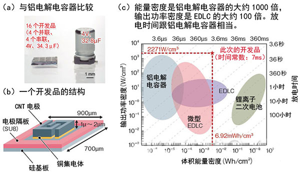
Figure 1: The charge and discharge times are much shorter than the conventional double layer capacitors
A unit consisting of 4 and 4 strings of 16 IEDCs is compared with an aluminum electrolytic capacitor with the same working voltage and electrostatic capacity (a). The volume is only about 1/838 of the aluminum electrolytic capacitor. The structure and size of an IEDC (b ). Compared with aluminum electrolytic capacitors, various electric double layer capacitors (EDLC) and lithium ion secondary batteries (c). The charge and discharge time is the same as that of an aluminum electrolytic capacitor and it is very short in EDLC. (The photo shows the Nikkei Technology Online based on the data of the Japan Institute of Technology)
The production of high-purity CNTs uses the “Supergrowth (SG) method†developed by ZTE, with a purity of 99.98%. The SG method has reached the mass production level. Japan Zeon Corp. will begin mass production in the second half of 2015.
IEDC's production uses photolithography that can be mass-produced (Figure 2). The CNTs were dispersed in an aqueous solvent to make a CNT paste, which was then painted with a razor blade onto a patterned gold collector. Then, the CNT layer is processed into the same shape as the gold collector by photolithography and etching. This time, using this process, 4,700 IEDCs were manufactured on a 4 inch (about 100 mm) silicon wafer.
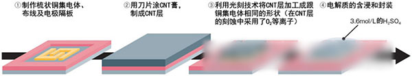
Figure 2: CNT layer made by photolithography
Outline of the IEDC manufacturing process: (1) The U-shaped gold current collectors were combined into a comb-like shape, and then an electrode separator was fabricated using an epoxy resin (SU8) that is highly water-repellent against electrolyte dilute sulfuric acid. (2) A CNT paste is applied thereon with a blade, and (3) a CNT layer is formed using photolithography and etching techniques. This time, dilute sulfuric acid was used as the electrolyte. (The picture shows the Nikkei Technology Online based on the information produced by the Institute)
100V withstand voltage is also very easy to achieve
The advantages of mass production on silicon wafers include, in addition to mass production, the fact that it is easy to achieve series and parallel connection of multiple chips, and it is possible to design operating voltage and electrostatic capacity with a high degree of freedom. The changes in voltage and capacitance caused by series and parallel connections are "almost the same as in textbooks," says Kenji Kenji, head of the Institute of Applied Nanotubes Practical Research Center.
For example, if a single chip has a withstand voltage of 1 V and an electrostatic capacity of about 30 μF, such four chips are connected in series and connected in parallel, and a device with a withstand voltage of 4 V and an electrostatic capacity of about 30 μF can be realized (Fig. 1(a)) ). If 100 chips are connected in series, a withstand voltage of 100V can also be achieved. By connecting 100 chips in parallel, a capacitance of about 3000 μF can be achieved.
Available for AC-DC conversion
The IEDC also has some issues. First, the equivalent series resistance (ESR) is greater than that of an aluminum electrolytic capacitor. In general, larger ESR is not suitable for high frequency and high current applications. Even so, the company said that it has confirmed that the IEDC can work normally in low-frequency applications such as 60-Hz AC-DC conversion.
Of course, ESR is also good. Because of the small size of the MLCC that competes with IEDC, there is a problem that the ESR is too small to oscillate.
Another topic of IEDC is high manufacturing cost (Figure 3). The reason is that the cost of the lithography apparatus is high, but Kenji Kensai stated that "the unit price may drop to around 100 yen, which is almost the same as when MEMS (micro-electro-mechanical-system) components were first mass-produced."
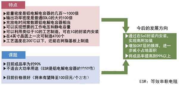
Figure 3: Future costs will be comparable to MEMS components
IEDC's characteristics, topics and future development direction. Due to the use of lithography technology, even if the cost is reduced, the individual cost is around 100 yen, which is comparable to MEMS and still higher than that of aluminum electrolytic capacitors. On the other hand, the IEDC has additional values, such as mounting in a SoC package, manufacturing on a resin substrate, and the like. In the future, further miniaturization is expected, and the yield rate will also increase.
High cost offset by high value-added
The hope of ITRI's development of the IEDC is to find new uses that can make full use of its added value and put it into practical use instead of competing with existing products for price competition.
In the future, Zynq will further reduce the chip size by increasing the film thickness of CNTs, and at the same time increase the current yield of about 90% to 99% or more, and realize practical application. Kenji Kensai stated that "it is also intended to replace the Si substrate and manufacture IEDC on the resin substrate to reduce its cost and expand its use." (Reporter: Nozawa Tetsuo)
Pentaerythrityl Tetrastearate,Cas 115-83-3,Pentaerythrityl Tetrastearate Cas 115-83-3,Pentaerythrityl Tetrastearate 115-83-3
Jiangxi Zhilian Plastics & Chemicals Technology Co., Ltd , https://www.zhilian163.com